Description
Custom two-channel USB audio interface centered around an ALINX AC7Z010 Zynq-7000 system-on-module. Intended as a full mixed-signal hardware and embedded-systems design exercise: analog instrument/line input circuitry, audio ADC clocking, FPGA-based I2S capture, Linux USB Audio Class 2 streaming, display/UI integration, and real-time effects control capabilities.
The first revision targets a self-powered 24-bit / 48 kHz USB Audio Class 2 capture device with an integrated ST7789 display for metering, USB status, sample-rate display, and clipping indication. The core signal path is:
Architecture:
- 1/4" TRS input
- ESD/RF protection
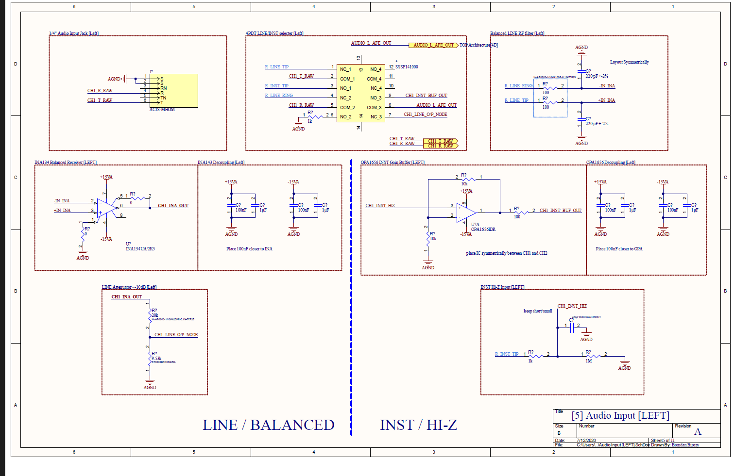
- Selectable Hi-Z instrument or balanced line input stage
- OPA1656 ADC driver/filter
- CS5361 stereo audio ADC
- 24-bit I2S into Zynq programmable logic
- Async FIFO / metering / DMA
- Zynq processing system running Linux UAC2 gadget
- USB-C USB 2.0 high-speed device connection
The analog front end is being designed to support both electric guitar/bass-style Hi-Z instrument input and balanced TRS line input. Instrument mode uses a high-impedance FET-input buffer path, while line mode uses an INA134-style balanced receiver with matched RF filtering and appropriate level scaling before the ADC driver. The CS5361 is clocked from a dedicated 24.576 MHz audio oscillator and runs as the audio clock master, generating 48 kHz LRCK and 3.072 MHz SCLK for the FPGA I2S receiver. The original project scope defines this as a 24-bit, 48 kHz UAC2 capture interface with ST7789 display support and later effects hooks.
On the FPGA side, I am implementing the I2S receive path in the ADC clock domain, sign-extending 24-bit stereo samples into 32-bit containers, crossing into the AXI clock domain through an asynchronous FIFO, and exposing audio data to the Zynq PS through DMA. Metering logic will compute peak/RMS levels and clip flags in hardware, with status registers exposed to Linux and the display UI. The design intentionally reserves a future DSP/effects slot after the capture path is stable rather than adding effects before the base audio path is validated.
The processing-system side uses embedded Linux on the Zynq ARM cores. The planned software path is to first bring up USB device mode, then configure a USB Audio Class 2 capture gadget, then connect the FPGA DMA stream to the capture endpoint. Because the ADC audio clock is independent of the USB host clock, the design is planned around asynchronous UAC2 capture rather than assuming the USB host and ADC clocks are perfectly locked.
Final design will incorporate detachable external effects control surface. The main audio interface board will include a UART-based expansion port for a future Teensy 4.1-powered controller panel. The main board’s display and onboard controls select the active effect or parameter page, while the detachable control surface provides physical knobs, buttons, and encoders for real-time parameter adjustment. The Teensy 4.1 will scan the external controls locally, handle debouncing and encoder/pot filtering, and transmit compact UART control packets to the Zynq system. This keeps raw potentiometer and button wiring off the main mixed-signal board and avoids routing noisy control lines near the ADC, audio oscillator, Hi-Z input nodes, and analog reference circuitry.
The UART expansion interface is being designed as a low-speed digital control link rather than an audio path. The detachable panel will be powered separately or through a protected auxiliary power pin, with shared ground reference, UART TX/RX, panel-detect, reset, and optional interrupt/status lines. The main carrier will treat the Teensy panel as a removable human-interface device: if the panel is attached, the Zynq software accepts parameter updates from it; if absent, the interface remains fully usable through the onboard display and controls.
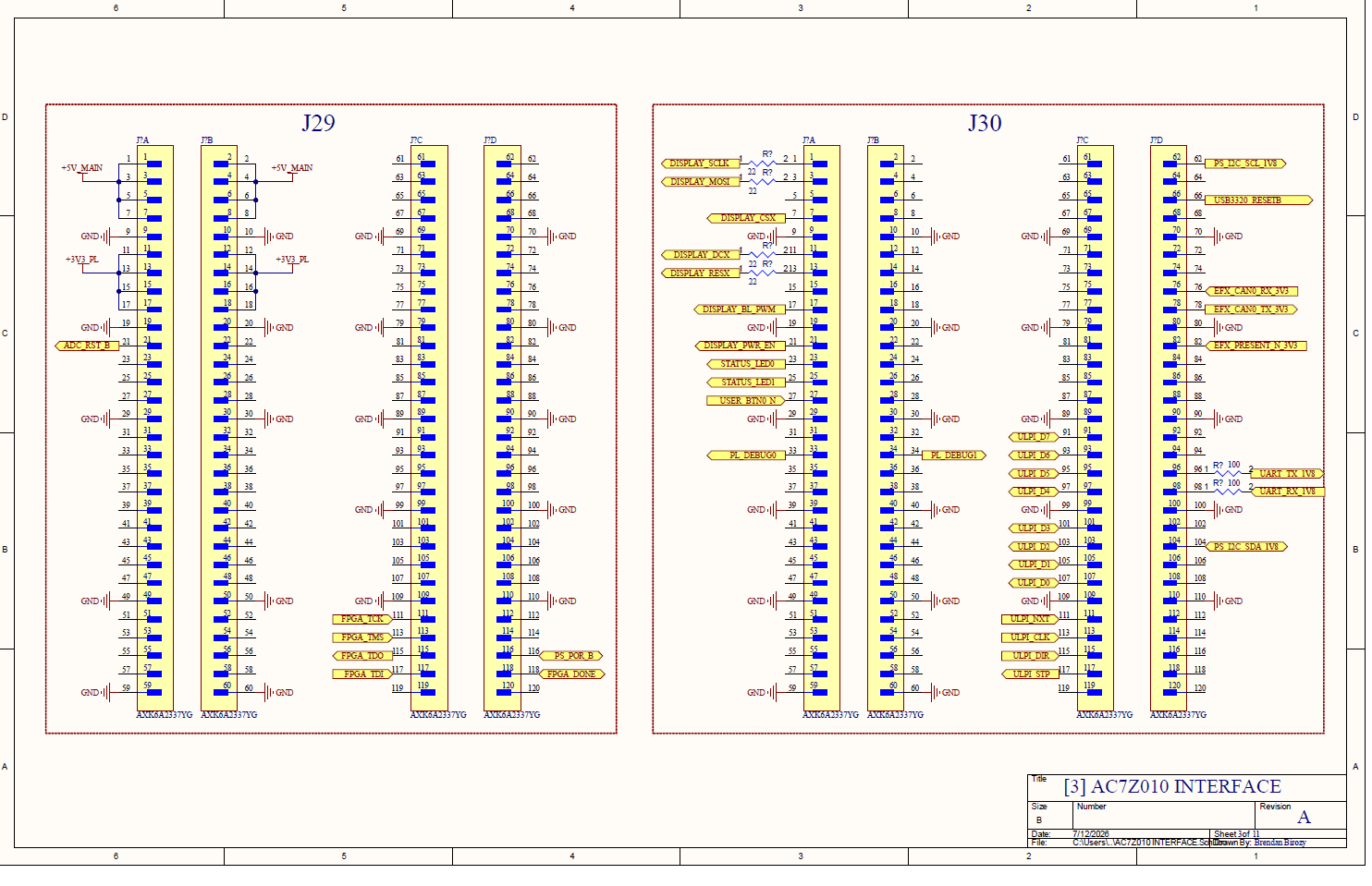
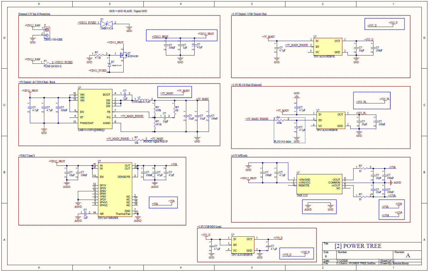
The PCB is planned as a four-layer carrier board with a continuous ground plane, separated analog/digital placement domains, local filtering, and test points for critical power, clock, audio, USB, and debug signals. The power architecture is self-powered from an external 12 V DC input, with USB-C VBUS used only for attach/sense rather than as the main board supply for design simplicity. The wiring plan locks the board as a complete AC7Z010 carrier, with external 12 V input, clean analog rails, digital rails, USB PHY support, display support, and JTAG.
... ...
Progress Captures as of 7/17
All designs are preliminary previews.
Audio Channel:
Power Tree Architecture:
FPGA SoC Interface: